Why polarization state reveals the target
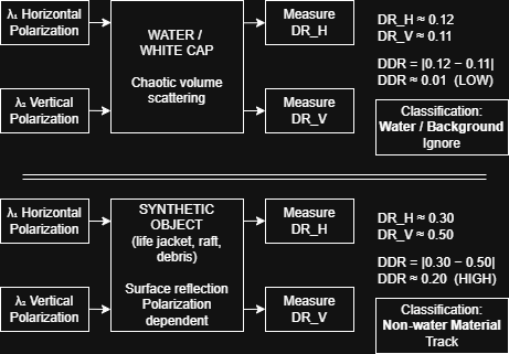
When laser light scatters from a surface, the polarization state of the return depends on the structural symmetry of the scattering medium. Isotropic media — like open ocean water — scatter without preferential polarization direction, producing returns where both orthogonal polarization channels carry approximately equal energy.
Biological tissue is not isotropic. Skin, subcutaneous fat, wetsuit neoprene, and synthetic life vest materials are all built from layered, fibrous, or anisotropic structures that scatter preferentially along one polarization axis. The DDR measurement captures this asymmetry directly as a ratio of the two orthogonal return amplitudes.
The ocean background presents DDR ≈ 0. Biological and synthetic targets present DDR > 0, with approximately 20:1 contrast against the sea surface under all tested sea states up to Beaufort 4.
| Ocean water DDR | ≈ 0.0 (isotropic scatter) |
| Biological tissue DDR | 0.15 – 0.35 (anisotropic structure) |
| Neoprene wetsuit DDR | 0.20 – 0.40 |
| Life vest material DDR | 0.25 – 0.45 |
| Contrast ratio | ≈ 20:1 against sea surface background |
From photons to classification in a single pipeline
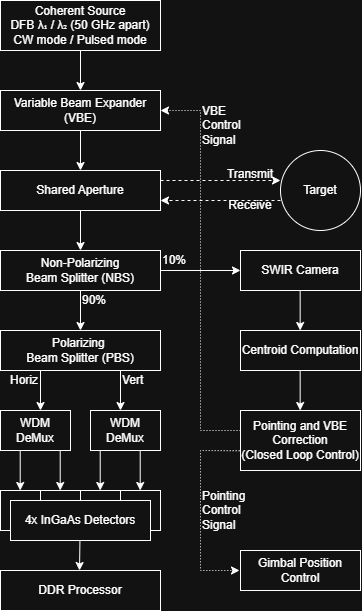
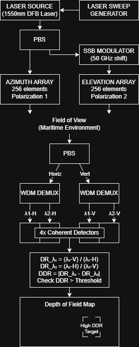
DDR processing uses dual-wavelength coherent detection at 1550nm with FMCW ranging. The transmitted beam passes through a polarizing beam splitter before illuminating the target; the return passes through a second orthogonally-oriented splitter, separating it into H and V polarization channels for simultaneous coherent detection.
FMCW modulation provides range gating, allowing the system to bin returns by slant range and reject clutter from rain, spray, and sea surface specular returns that arrive at the wrong range gate. The DDR ratio is computed per range bin per scan line, producing a 2D map of depolarization asymmetry over the search zone.
| Wavelength | 1550nm (eye-safe Class 1M) |
| Ranging modality | FMCW (frequency-modulated continuous wave) |
| Detection | Balanced coherent, dual-channel (H + V) |
| Operating range | 300m – 5km |
| DDR computation | Per range-bin, per scan line, real-time |
| Output | Scalar classification flag, no image required |
Dual 1D silicon photonic phased arrays
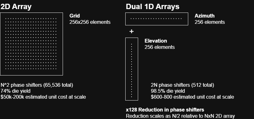
The transmit and receive apertures each use a 256-element silicon photonic phased array fabricated on a standard 200mm CMOS-compatible process node. The array steers a collimated 1550nm beam in one axis electronically; the second steering axis is achieved mechanically via a single-axis galvo mirror. This 1D architecture was selected specifically for its manufacturing yield advantage.
A 2D phased array of equivalent aperture requires a 256×256 element grid — 65,536 elements per die — with all elements and their drive circuits within the die area. Yield falls approximately as the square of the 1D yield for the same defect density. A 1D array with 98.5% yield per device produces a 2D equivalent with approximately 74% yield. Twenty 1D dies occupy the same wafer area as one 2D die, and post-test pairing of H and V arrays further improves matched system yield.
| Array architecture | 1D, 256 elements per axis |
| Fabrication node | 200mm, CMOS-compatible silicon photonics |
| 1D array yield | ~98.5% per device at mature node |
| Equivalent 2D yield | ~74% (256×256 element grid) |
| Wafer density advantage | 20× 1D dies per equivalent 2D die area |
| Target volume unit cost | $600 – $800 vs $50,000 – $200,000 (2D) |